
What if the MSX would have an USB connection? And if the BIOS/MSX DOS would automatically recognize devices connected to it?
Inspired by the work of Xavirompe and his RookieDrive, S0urceror started a project to do exactly that. Provide an USB interface to MSX computers. On his GitHub repository you can find:
- Schematics (KiCAD), that interfaces a cheap USB CH376s board to the MSX cartridge port.
- Drivers, currently Flash drives on Nextor and HID keyboards are supported.
- Debugging tools, to connect a test board to your PC/MAC and assist in debugging.
I’ve been engaged with S0urceror and Issalig (another active collaborator) to improve the project. My contributions were to review the code and perform changes to support more pen drives as well as solving a few bugs. Recently I also decided to invest some time to improve the PCB and the Verilog code that implements the ROM mapper so we can get some new features.
This blog post is to document the steps I took to improve the project, including pointers to the BOM and the new PCB created for it.
Everything is available on my GitHub MSXUSB fork repo cristianoag/MSX-USB: Schematics, drivers, debug tools, to make USB devices on the MSX a reality (github.com) or in the original GitHub repo maintained by S0urceror S0urceror/MSX-USB: Schematics, drivers, debug tools, to make USB devices on the MSX a reality (github.com)
If you are a video person, please check the video below that has a summary of this article. Although it is in Portuguese, you can always enable translated closed captions on YouTube and have fun with the mistakes. 🙂
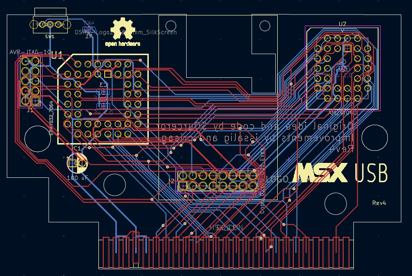
The new PCB
The first version of the PCB created by S0urceror was planned to use a flash (SST39SF040) in its DIP version and an Altera CPLD (EPM7064SLC44) in it PLCC44 version. Below you can see a picture of his PCB.

It worked ok, but had a few problems. The main issue was with the excessive high profile of the sockets used that made impossible to enclose the PCB inside any standard MSX cartridge case. I ended up creating a case with a squared hole to allow at least closing it and make easier to connect/disconnect to my MSX computers.

Then Issalig made a review of the board that also worked great. It is smaller but with another annoying issue. The place to connect the CHS376 module was located on the edge of the board, and when enclosing it in a cartridge case, part of the module PCB is exposed.

I made a 3D printed case for Issalig’s board, but as you can see below, it is ugly when you can see part of the electronics outside.

I then decided to create a new version of the PCB, this time allowing the right enclosure if using lower PLCC sockets and positioning the CHS376 module in the right place to have the connector correctly exposed at the edge of the cartridge. I also decided to go one step further and include a toggle switch to allow us to decide which 128K image we will load when booting with the cartridge.

The toggle is basically selecting between the first two 128K roms stored on the flash memory. It doesn’t matter if you are going to use a 512K or 256K version of the flash, you will need to flash the first two 128K slots (first 256K) with two images of the software.
I’m doing that to allow the use of the MSXUSB-NXT version of the code, that allows us to load software from the pen drives inserted into the cartridge and the MSXUSB traditional software that allows us to load USB devices like keyboards and ethernet cards to the MSX computer.
Here is the 3D model of the PCB already with a hole to host the USB module appropriately.

Changes to the Verilog code (CPLD)
The verilog code had to be changed to support the toggle switch. Checking the code you can see the Konami SCC mapper is being used to load the ROM file stored on the flash into specific memory banks defined by the mapper specification.
The two first 128K slots of the flash are selected by the bit 17 from the 19 bits available (0-18). Changing the bit 17 to 0 we instruct the mapper to load from the beginning of the flash, changing it to 1 the load will start from 128K until 256K.
So we changed part of the mapper code to control that bit depending on the value mapped to the pin 2 of the CPLD. In Quartus I had to define pin2 to the correct rom_sl signal I created on the Verilog code.
Here is a picture of the prototype I used to test the new Verilog code on my computer. You can also check it working on the video I mentioned earlier.

How to build your own MSX-USB?
Issalig created a great set of instructions to guide during the process to build the MSX-USB board, program the CPLD and the flash memory. You can check all instructions on his GitHub fork here issalig/MSX-USB: Schematics, drivers, debug tools, to make USB devices on the MSX a reality (github.com)
The new PCB board has additional components that are needed to support the new pull-up/down circuit used to control the flash memory load.
On the following sections you can find the updated Bill of Materials (BOM) as well as a copy of Issalig’s instructions showing how to program the CPLD and the flash memory.
PCB
You can download the latest version of the printed circuit board gerber files from my GitHub repository here. Then you need to order a set of PCBs from one of the well-known PCB manufacturers out there. You will need to provide them the zip file you downloaded from GitHub and pay for the fabrication.
Bill of Materials
Here is the list of materials required to build the MSXUSB cartridge.
| References | Values | Footprint | Qtd | Link |
| C2, C3, C4 | 100 nf (0.1 uf) | C_0805_2012Metric_Pad1.18×1.45mm_HandSolder | 3 | Ali Express |
| C1 | 100 uF 10V | CP_Radial_D5.0mm_P2.50mm | 1 | Ali Express |
| R1 | 4K7 | R_0805_2012Metric_Pad1.20×1.40mm_HandSolder | 1 | Ali Express |
| U1 | EPM7064SLC44-10(*) | PLCC44 | 1 | UTSource |
| U2 | AM29F040B-70JC | PLCC-32_THT-Socket | 1 | Ali Express |
| SW1 | SK-12D07VG4 | SK12D07VG4 toggle switch (small) 90 degrees | 1 | Ali Express |
| Module | CH376S | CH376S U Disk Read Write Module Supports USB Control Transfer 12MHz | 1 | Ali Express |
| Socket 1 | PLCC 32 DIP | Low profile DIP PLCC Socket adapter | 1 | Ali Express |
| Socket 2 | PLCC 44 DIP | Low profile DIP PLCC Socket adapter | 1 | Ali Express |
(*) You can also use ATMEL’s ATF1504AS instead. Just make sure to read the instructions below if you decide to use that one.
Step 1: Program CPLD
You will need the obsolete part EPM7064SLC44-10. You can get them from AliExpress and other places but as they are refurbished/recovered from dumpsters expect to have only 50% working, so order double if you decide to go with Ali Express. I provided links to UTSource on the table above as they are able to provide units from new old stock.
You will also need an Altera programmer such as USB blaster. You can purchase those from Ali Express or any other electronics shop around. You will use it to program the CPLD.
Next, you have to download Quartus software version 13.0sp1, as newer versions do not support EPM7064. Go to https://fpgasoftware.intel.com/?edition=lite and proceed with the download and installation.
Connect the programmer to the board and also power the board externally with 5V, you can do it using the expansion header or CH3786 header. Find the pins VCC and GND and you are done. Failing to do so it will result in an JTAG read error.
Next, we check your connection and if everything went ok you will see this message.
$ ./quartus_pgm --auto
Info (213045): Using programming cable "USB-Blaster [3-1]"
1) USB-Blaster [3-1]
  070640DD   EPM7064S

Info: Quartus II 32-bit Programmer was successful. 0 errors, 0 warnings
    Info: Peak virtual memory: 127 megabytes
    Info: Processing ended: Sat Dec 18 10:16:56 2021
    Info: Elapsed time: 00:00:00
    Info: Total CPU time (on all processors): 00:00:00
And it has arrived the amazing moment where you are going to program it (you can do it with the command line quartus_pgm or with the GUI tool quartus) with the following file: MSX-USB/MSXUSB.pof at master · cristianoag/MSX-USB (github.com)
./quartus_pgm -m jtag -o "p;./MSXUSB.pof"
In case the devices still shows JTAG communication error, keep calm and go to the next step.
Step 1b. Recovering dead JTAG units
It happens that some of the refurbished units come with programs that used JTAG pins for I/O and they are not able to be used for JTAG. I threw some of them to the bin until I discovered a recovery process (https://www.eevblog.com/forum/fpga/atmel-atf150x-cpld-and-wincupl/msg3162224/#msg3162224).
- Apply 12V to CPLD pin OE1 (44) with a 2k2 resistor for a minute or so. In my pcb you can access OE1 pin on header pin 15 (RST).
- Disconnect 12V, connect 5V and try to program it.
- Hopefully some CPLD’s are working now!
Step 1c. Use an still in production CPLD, use a ATF1504AS
As seen in https://www.eevblog.com/forum/fpga/atmel-atf150x-cpld-and-wincupl/msg3113922/#msg3113922 ATF1504AS is pin compatible to EPM7064 and it is a valid replacement for EPM7064. The changes are not that big: we will need to convert .pof into .jed and then into .svf.
I compiled the following info from different sources https://github.com/marqs85/snes_dejitter/blob/master/README.md, https://github.com/SukkoPera/OpenAmiga500FastRamExpansion/blob/master/firmware/README.md and https://www.hackup.net/2020/01/erasing-and-programming-the-atf1504-cpld/
All the resources for ATMEL CPLDS can be found at https://www.microchip.com/en-us/products/fpgas-and-plds/spld-cplds/pld-design-resources
First we need to download pof2jef from http://ww1.microchip.com/downloads/archive/pof2jed.zip Then in winpof2jed.exe (yes it works with wine in linux :))
1. Select .pof file from previous step as input file
2. Select 1504AS as device
3. Change the following options:
  * Reduce MC power -> On
  * Open Collector -> Off
  * JTAG mode -> On
  * Slew rate -> Slow
4. Click "Run"
The important thing here is JTAG Mode ON, if you are wrong you will block JTAG but don’t panic, we already know that applying 12V it will be enabled again.
Once we have the .jed file it is time to generate svf with ATMISP that you can download it from http://ww1.microchip.com/downloads/en/DeviceDoc/ATMISP7.zip. Then, you should follow these steps.
1. Create a new device chain via File->New
2. Set number of devices to 1
3. Set device to ATF1504AS
4. Set JTAG instruction to "Program/Verify"
5. Select .jed file from previous step as JEDEC file
6. Name your svf file
7. Click "OK"
8. Tick "Write SVF file" and click "Run"
We are almost there. We just need to flash it with openocd
But first we need the config file for usbblaster and you can save it as altera-usb-blaster.cfg
#
# Altera USB-Blaster
#
# http://www.altera.com/literature/ug/ug_usb_blstr.pdf
#

interface usb_blaster
usb_blaster_lowlevel_driver ftdi
# These are already the defaults.
# usb_blaster_vid_pid 0x09FB 0x6001
# usb_blaster_device_desc "USB-Blaster"
adapter_khz 3000
And this is the magical line that will flash your CPLD (Do not forget to power usbblaster with external 5V)
openocd -f altera-usb-blaster.cfg -c "adapter_khz 400" -c "transport select jtag" -c "jtag newtap ATF1504AS tap -irlen 3 -expected-id 0x0150403f" -c init -c "svf msxusb.svf" -c "sleep 200" -c shutdown
If everything went ok you will see something ending like this
Time used: 0m12s613ms
svf file programmed successfully for 3299 commands with 0 errors
shutdown command invoked
Step 2. Flash memory
The recommended memory chips is SST39SF040 (512kb) but I also managed to make it work with SST39SF020 (256kb). Then, you will need a programmer such as TL866 II https://aliexpress.com/item/33000308958.html and build the file for the newer MSXUSB revision using the following steps:
Download the file located at https://github.com/S0urceror/MSX-USB/blob/master/drivers/NextorUsbHost/dist/nextor.rom and rename it as nextor_1.rom.
Download the file located at https://github.com/S0urceror/MSX-USB/blob/master/drivers/NextorUsbHost/dist/nextor.rom and rename it as nextor_2.rom
Now you need to combine those two files into one. If you are using Windows, just execute:
copy /b nextor_1.rom+nextor2.rom nextor.romNow you need to program your flash chip with the nextor.rom file you just created.
If you prefer to use a command line tool I suggest you minipro https://gitlab.com/DavidGriffith/minipro
$ ./minipro --device SST39SF040@PLCC32 --write nextor.rom -s
Found TL866II+ 04.2.126 (0x27e)
Warning: Firmware is newer than expected.
  Expected  04.2.124 (0x27c)
  Found     04.2.126 (0x27e)
Chip ID OK: 0xBFB7
Warning: Incorrect file size: 131072 (needed 524288)
Erasing... 0.40Sec OK
Writing Code...  26.38Sec  OK
Reading Code...  4.00Sec  OK
Verification OK
Step 3. Prepare a disk
Once we are here, all the hardware requirements are fulfilled. It is only a matter of creating a disk image with the system files provided at https://github.com/S0urceror/MSX-USB/tree/master/software/dist
- If you have a MSX1 (i.e. VG8020, …) you will be limited to 720kb disks and FAT12. Do not complain, do you still prefer a slow datacorder? To create a MSX disk image I use dsktool from https://github.com/nataliapc/MSX_devs/tree/master/dsktool
I also provide linux and windows version of dsktool in order to make it easier, you can get them at https://github.com/issalig/MSX-USB/tree/master/software/utils
#create disk
dsktool c MYDISK.DSK
#add system files
dsktool a MYDISK.DSK COMMAND.COM MSXDOS.SYS
#add other files
dsktool a MYDISK.DSK MYGAME.COM
In case you prefer a GUI program you can also use DiskMgr http://www.lexlechz.at/en/software/DiskMgr.html
Next, flash it. Warning: check if your device is /dev/sda or you will destroy something. If you are a windows user maybe Rufus can write the image, if it works, please report it.
sudo dd if=MYDISK.DSK of=/dev/sda
- If you are a lucky MSX2 owner you will need a FAT16 partition of 16Mb with COMMAND2.COM and NEXTOR.SYS.
In Linux I have created an image available at https://github.com/issalig/MSX-USB/blob/master/software/utils/msx2.zip. You can do it with the following commands.
#create a 16 Mb disk and format it to FAT16
sudo  dd if=/dev/zero of=msx2.dsk bs=1024 count=16k
sudo mkfs.fat -F 16 msx2.dsk

#mount it
mkdir 16mb
sudo mount -o loop msx2.dsk 16mb/

#copy all the stuff
sudo cp COMMAND2.COM NEXTOR.SYS 16mb

#unmount it and flash it
sudo umount 16mb
sudo dd if=msx2.dsk of=/dev/sda bs=16M
You can also just format the USB stick with FAT16 and copy the MSXDOS/Nextor files directly to it, together with ROM or DSK games you like.
Unplug the stick from the computer, plug it in the MSXUSB, switch on the MSX and you are in. Enjoy!